Inverting And Combining An Open-Drain Signal
Lately, I have been working with the LTC4151-1 chip by Linear Technology. It is used to measure voltage and current with high resolution typically in telecommunications equipment. In the process of validating my design, I need to test it with the simplest circuit possible in order to simplify fabrication and eliminate variables introduced by other intermediate devices (namely, the required optoisolators).
The LTC4151-1 chip communicates over the I2C bus. Only problem: its setup breaks out the SDA (serial data) signal into SDAI (data in from the microcontroller) and /SDAO (data out to the microcontroller, inverted). It is broken out like this (with SDAO inverted) so that people can conveniently wire up optoisolators to reconcile different ground potentials that exist between the MCU and the unit whose voltage is being measured. (Many times, the V- out of the battery will not be the same as the GND used by your microcontroller logic, computer, or etc., especially if you are measuring individual batteries within strings of batteries.) In order to combine the lines, I could have tied the /SDAO line to a 7404 inverter and added a pull-up resistor so the line is pulled high when the /SDAO line goes high-impedance before coming to the inverter. Normally this would be OK because I2C signals are never driven high; they are only driven low and to high-impedance. However, in the event that SDAI was being pulled low at the same time /SDAO was also being pulled low, this would cause the output of the inverter to go high, likely resulting in a nasty short circuit and/or bus contention. Let's try to avoid this situation, even if it is unlikely to happen unless there is an error.
Basically, what I need to build is a NOR gate with one inverted input. As SDAI goes low or /SDAO goes high, the output signal is supposed to go low as well.
In this case, I will define the master device as my microcontroller and the slave device as my LTC4151-1 chip.
Here's how you do it. You will need one NPN transistor and jumper wires. I used a common 2N3904 which you should have if you collect parts.
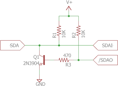
- Connect SCL from the slave device to the master device, then to a pull-up resistor. (Since this is the standard arrangement, it is not shown in the schematic below.)
- Connect SDAI from the slave device to the collector of an NPN transistor, then to a pullup resistor.
- Connect /SDAO from the slave device to the base of an NPN transistor, then to a pullup resistor.
- Connect the emitter of the NPN transistor to ground.
- Connect SDA from the master device to the collector of the transistor.
Here's what I just described with the bullets, in picture form. Note that GND in the schematic must be shared across all your devices, as described in the next paragraph. Also, the resistor values are not guaranteed to work in every situation, but worked for me with my LTC chip. Ohm's Law is your friend, especially if your devices need a particular amount of current for them to be responsive.
Most importantly, since the LTC4151-1 can measure voltage across its ground pin and a pin called VSENSE+, its ground pin must be tied to the same ground as the microcontroller and the transistor or else the circuit will not work. When I have this configuration hooked up to my laptop for serial verification of data, I use the USB ground pin as the ground to my microcontroller, the transistor, and the USB chip, and I hook up this ground to the negative terminal of the cheap drugstore 9V battery I use for testing the LTC chip.
This works because when the base is on (i.e. /SDAO is being pulled high by the pullup resistor and data is being transmitted), the current flows through the transistor with no resistance, and since the emitter is grounded, this pulls the whole SDA signal low. When the base is turned off, this turns the transistor into an open switch, thus forcing the SDA signal to be pulled up by the pullup resistor. And, of course, when the SDA pin from the master device is getting pulled low, this still grounds out the SDAI signal on the slave device because the collector is low and won't have any voltage difference from ground anyway, even if the transistor's base gets turned on.
Having trouble finding the address of your I2C device?
Have a look at this brilliant blog post "I2C Scanner" by Nick Gammon on his forum. It is Arduino code you can use to iterate through all possible I2C devices and see which one(s) return a response. www.gammon.com.au/forum/?id=


Comments
Post a Comment